ABSTRACT
Two-dimensional van der Waals (2D vdW) magnets have attracted enormous attention as an emerging material platform for magnetism, spintronics, and multifunctional applications. Their single-crystalline layered structures, layer-number controllability, and unique 2D properties provide unique opportunities that are difficult to achieve in conventional magnetic materials. However, the discovery and development of new 2D magnetic compounds require considerable time and effort, and only a limited number of these materials have been reported to be suitable for practical use. Therefore, materials engineering based on already established 2D vdW magnets has become an important research direction to explore new characteristics and find a practical route for device applications. This review summarizes recent materials engineering pathways for 2D vdW magnets. The main contents focus on the engineering strategy through electrostatic, chemical, lattice, symmetry, and heterostructure ways. These approaches provide practical design routes for tailoring magnetic properties beyond intrinsic 2D vdW magnets. Further progress will require broader application to various types of materials and delicate optimization that connects expanding fundamental magnetism with electromagnetic device applications.
-
KEYWORDS: Two-dimensional van der Waals magnet, Magnetism, Spintronics, 2D engineering
1 Introduction
Magnetic materials have played an important role in modern electronic technologies for magnetic sensing, information storage, actuation, and multifunctional device applications. In conventional magnetic materials, the magnetic properties are mainly determined by chemical compositions and structures. In contrast, two-dimensional van der Waals (2D vdW) magnets provide different types of approaches as they are composed of monolayers having strong intralayer coupling but weakly coupled through interlayer interactions. This enables the material to be easily exfoliated, stacked, and integrated with various types of 2D vdW layers for on-demand device architectures.
The field of 2D vdW magnetism has been rapidly growing since the first experimental discovery of intrinsic 2D magnetism in atomically thin layers such as Cr
2Ge
2Te
6 and CrI
3 [
1,
2]. Since then, various 2D magnetic materials have been investigated, including the metallic ferromagnet Fe
3GeTe
2 [
3], antiferromagnetic semiconductors MPX
3 [
4] and CrSBr [
5], magnetic topological materials MnBi
2Te
4 [
6], etc. These materials exhibit diverse magnetic ground states, transition temperatures [
7], domain configurations [
8], and magnetic anisotropies [
9], which are particularly important for spintronic applications as they determine the stability and switching efficiency of devices. In addition, their single-crystalline layered nature and excellent layer-number controllability provide a route for constructing on-demand heterostructures, enabling not only the development of novel device platforms but also the exploration of new physics and materials science.
Despite these advantages, the development of 2D vdW magnets faces several limitations. A major challenge is that the discovery of new 2D magnets requires considerable effort for synthesizing compounds, single phase optimization, and spatial homogeneity. Moreover, only a limited number of 2D vdW magnets exhibit a room-temperature operation and air stability that are critical for practical device applications. Therefore, relying only on the discovery of new magnets may not be sufficient for rapidly expanding the use of 2D vdW magnets.
For this reason, materials engineering based on existing 2D vdW magnets can be an important research direction. Instead of developing entire material systems, materials engineering aims to reshape the magnetic properties of known compounds by modifying variables. This approach is a particularly effective way in 2D vdW systems because their atomically thin nature makes them sensitive to external perturbations.
In this review, recent progress in materials engineering of 2D vdW magnets is summarized from the viewpoint of controlling magnetic properties. This review emphasizes how established 2D vdW magnets can be modified and optimized through electrostatic, chemical, lattice, symmetry, and heterostructure engineering. Although these engineering methods are not completely independent, classifying them into individual pathways provides a useful framework for understanding how specific factors govern magnetic properties and emergent functional responses.
2 Materials Engineering for 2D van der Waals Magnets
2.1 Electrostatic Engineering: Dielectric, Ferroelectric, and Ionic Gate
Electrostatic gating is the most direct route to control the properties of 2D vdW magnets. Atomically flat and thin 2D crystals enable the efficient application of gate bias as they have high surface-to-volume ratios and small electrostatic screening lengths. The gate bias on magnets can modulate the magnetic anisotropy and exchange interaction through the control of carrier density, band filling, etc., without changing the chemical composition or structure of the material.
2D vdW antiferromagnets are excellent candidates for gate engineering. For instance, CrI
3 is a layered antiferromagnet, composed of ferromagnetic monolayers coupled antiferromagnetically. Electrostatic gates can switch the interlayer alignment between antiferromagnetic and ferromagnetic in CrI
3 through the spin-flip transition [
10,
11]. The microscopic origin is not simply carrier accumulation, but associated with interlayer exchange and the relative energy of competing magnetic states. Similar cases have been reported for other antiferromagnets, but through charge transport. Cr
2Ge
2Te
6 has exhibited the magnetic anisotropy control via electrostatic doping [
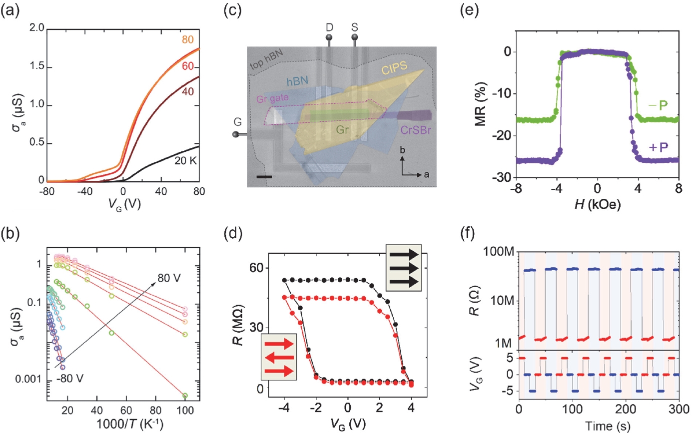
12]. CrSBr is an antiferromagnetic semiconductor having a narrower bandgap which enables carrier doping by electrostatic gating [
13], as shown in
Fig. 1(a,b). Moreover, the gate bias gives rise to the modulation of carrier-mediated magnetic anisotropy [
14]. Beyond conventional dielectric gating, nonvolatile electrostatic control has also been demonstrated in CrSBr by integrating ferroelectric and floating-gate architectures, respectively [
15]. In these devices, remanent polarizations or stored charges remain even after the applied gate bias is removed, enabling persistent modulation of the magnetic properties, as shown in
Fig. 1(c-f).
Ionic gating extends this concept to reach much higher charge densities than conventional solid dielectrics. The best-known case is the ferromagnetic Fe
3GeTe
2, where an ionic gate raised the ferromagnetic transition temperature close to room temperature in thin flakes, even though it was a metallic magnet [
3]. The mechanism relies not only on the electric double layer but also on ionic intercalation into the interlayer gap of the magnet, which maximizes the effective contact surface and resulting gating effects. It clearly demonstrates the strength of the gating in itinerant magnets, where the density of states near the Fermi level, exchange splitting, and magnetocrystalline anisotropy can respond strongly to carrier density [
16]. However, ionic gating also highlights a caution. The induced high carrier densities may be accompanied by structural changes through electrochemical reactions, ion migration, etc. The boundary between electrostatic carrier doping and chemical modification must therefore be carefully investigated to establish proper physics and methodologies.
Single crystallinity and vdW interlayer gaps make 2D vdW magnets ideal platforms for chemical engineering as they expose maximized accessible surfaces. As exchange interaction is often mediated by ligands and interlayer coupling across vdW gaps, chemical perturbations can strongly modify the magnetism of 2D magnets.
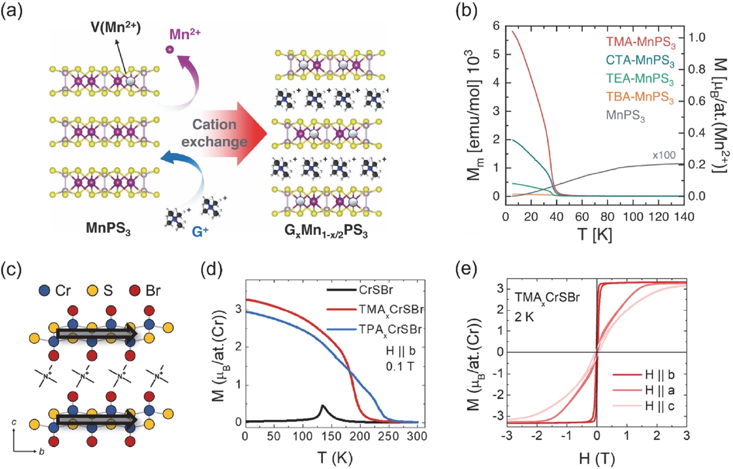
Chemical intercalation is particularly natural for layered magnets. Guest atoms, ions, or molecules can enter the vdW interlayer gap of a host magnet without destroying the intralayer framework. The guest species act as spacers, charge donors or acceptors, or local strain sources. For instance, organic intercalation converts MnPS3 from antiferromagnetic to ferrimagnetic through the modification of the molecule-dependent vacancy process (
Fig. 2(a,b)) [
17]. The chemistry of the guest species determines how vacancies form, how charge is compensated, and how the antiferromagnetic host is modified. CrSBr provides another representative illustration for controlling interlayer distance. Organic intercalation expands the vdW gap of CrSBr and drives a transition from antiferromagnetic to ferromagnetic order since the monolayer of CrSBr is ferromagnetic [
18]. In addition, the intercalated molecules simultaneously modify the interlayer exchange pathway which leads to the enhancement of the magnetic transition temperature (
Fig. 2(c-e)). This type of chemistry is more appealing as it allows magnetic modification not only in bulk crystals but also in thin flakes.
Defect engineering is another chemical route. Point defects and grain boundaries can introduce local moments, pinned magnetic domains, or additional exchange interactions. The difficulty is quantitative control of defects as a small number of defects could induce a random distribution which gives rise to misleading interpretation, especially in monolayer samples [
19,
20]. For this reason, defect-engineered 2D magnets should be carefully characterized through magnetometry, magnetotransport, and spectroscopy.
Compared with electrostatic gating, chemical engineering offers a more persistent change and a suitable route for a scalable process. At the same time, this methodology may introduce spatial inhomogeneity and structural degradation, highlighting the need to maintain the crystalline quality and long-range magnetic order of 2D vdW magnets.
2.3 Lattice Engineering: Strain and Pressure
Magnetism in 2D vdW materials is sensitive to lattice structures linked to the bond length and angle of adjacent atoms. This sensitivity arises because exchange coupling is strongly coupled to orbital overlap and crystal field splitting. Unlike the electrostatic and chemical approaches, strain and pressure directly modify the lattice structure of a target magnet.
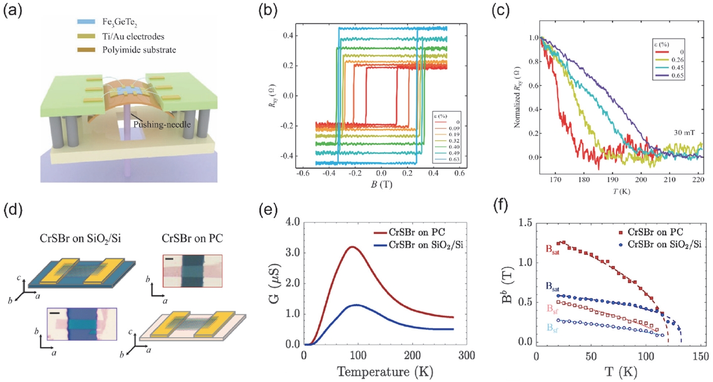
The application of strain to an Fe
3GeTe
2 thin film modulates the coercive field by more than 150% and even the Curie temperature, shown in
Fig. 3(a-c) [
21]. This is explained by the fact that the ferromagnetic order relies on the bonding of Fe-Ge-Te atoms and results in the change of magnetocrystalline anisotropy. CrSBr presents another example of the strain effect. The mechanical deformation induced by a substrate with different lattice parameters changes the electronic, magnetic, and optical properties of CrSBr (
Fig. 3(d-f)) [
22].
Hydrostatic pressure is another powerful route to control lattice structures. Unlike the uniaxial strain, the application of pressure mainly reduces the interlayer spacing of a target magnet and drives the rearrangement of interlayer exchange coupling. In atomically thin CrI
3, pressure induces a transition from antiferromagnetic to ferromagnetic interlayer coupling [
23].
Taken together, lattice engineering offers a direct route for designing on-demand structures and achieving magnetic properties in 2D vdW magnets. At the same time, spatially nonuniform distribution, in particular near the edge of a target magnet, remains an inevitable limitation for practical application. Therefore, comprehensive studies combining structural probes, spectroscopic analyses, and magnetometry measurements will be essential for lattice engineering.
2.4 Symmetry Engineering
Symmetry engineering is an emerging strategy to add electrical readout functions in 2D vdW magnets. Spatial inversion symmetry is a crucial factor which determines whether second-order nonlinear transport is allowed or forbidden. Once inversion symmetry is broken by layer number, stacking order, or an external electric field, nonlinear electrical responses can appear. This is directly linked to electronic applications since the nonlinear charge transport can convert an alternating current (AC) into a rectified direct current (DC) signal, providing a route toward AC-to-DC conversion for energy harvesting. In addition, the symmetry-controlled nonreciprocal transport can produce diode-like behavior, even in a simple two-terminal geometry. Therefore, symmetry engineering is not only a fundamental concept but also a practical design for electrically readable 2D magnetic devices.
The first demonstration of symmetry engineering has been reported in MnBi
2Te
4, a 2D vdW magnetic topological insulator. In an odd layer of MnBi
2Te
4, broken inversion symmetry enables second-order nonlinear transport associated with antiferromagnetic order [
24]. In contrast, even layers of MnBi
2Te
4, which preserve inversion symmetry, suppress the second-order response [
25].
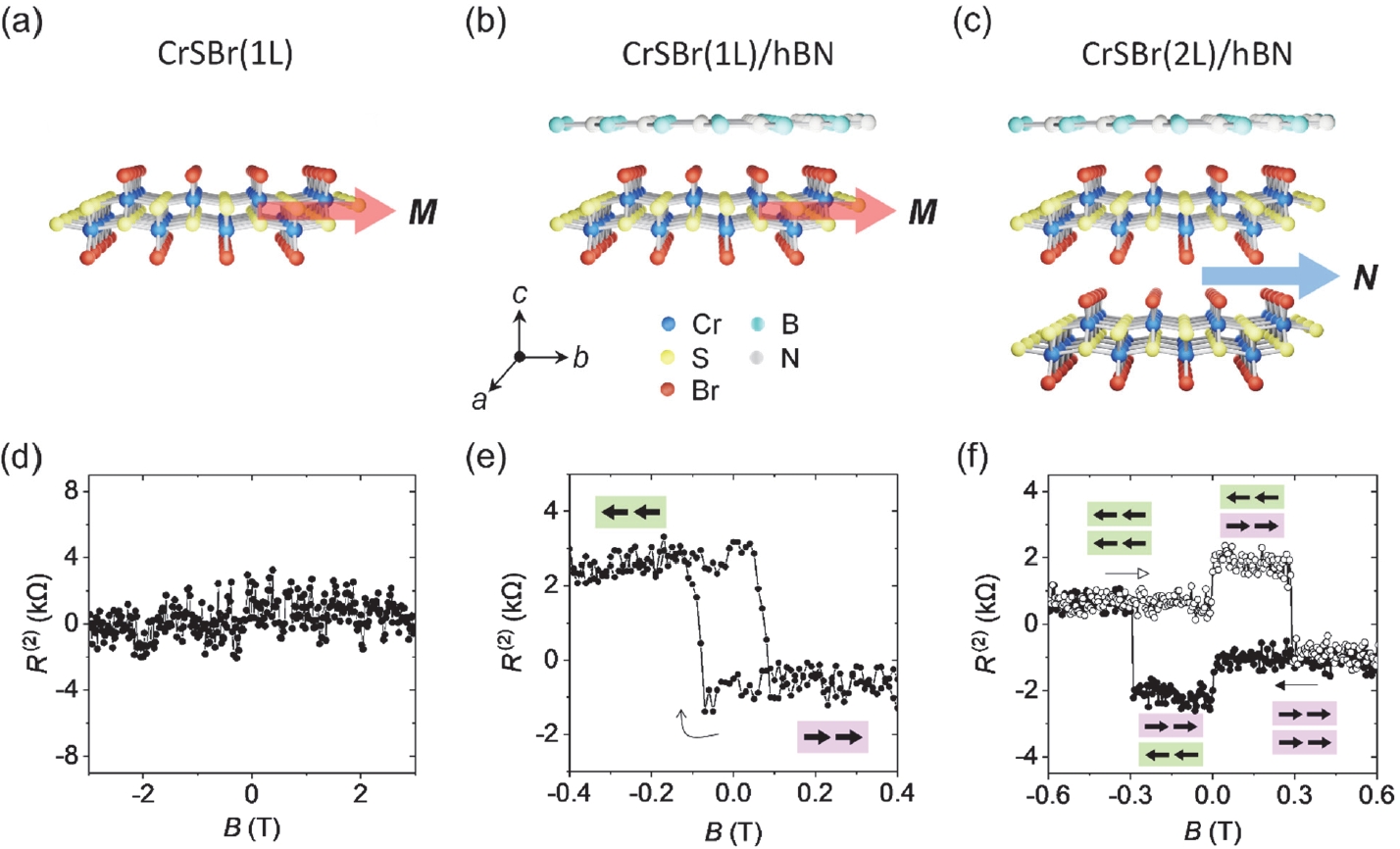
The study of 2D vdW magnet CrSBr offers a more practical approach for material design, as shown in
Fig. 4 [
26]. The report has demonstrated the practical symmetry engineering by the application of a hexagonal boron nitride layer on top to break the symmetry of CrSBr. In addition, since this nonreciprocal response is linked to the magnetic order of CrSBr, nonvolatile second-order responses controlled by magnetization and Néel vectors have been obtained. Thus, the control of structural symmetry provides an efficient route to activate the second-order response for electrically readable magnetic devices.
A heterostructure is the most general but powerful way to design new material systems, as it combines 2D vdW magnets with other layered materials to create properties that do not exist in either component alone. Unlike conventional thin film heterostructures, vdW materials can be stacked free from lattice mismatch constraints, allowing vdW magnetic layers to ideally combine with other vdW materials and other kinds such as molecular layers.
A representative example of 2D vdW layers is the CrI
3/WTe
2 heterostructure [
27]. When they couple through a clean interface, the proximity effect induces an exchange field to the WTe
2, which enables nonreciprocal charge transport. This demonstrates that vdW heterostructures not only alter the property of a magnet but also induce magnetic proximity to an adjacent nonmagnet, giving rise to a new type of material.
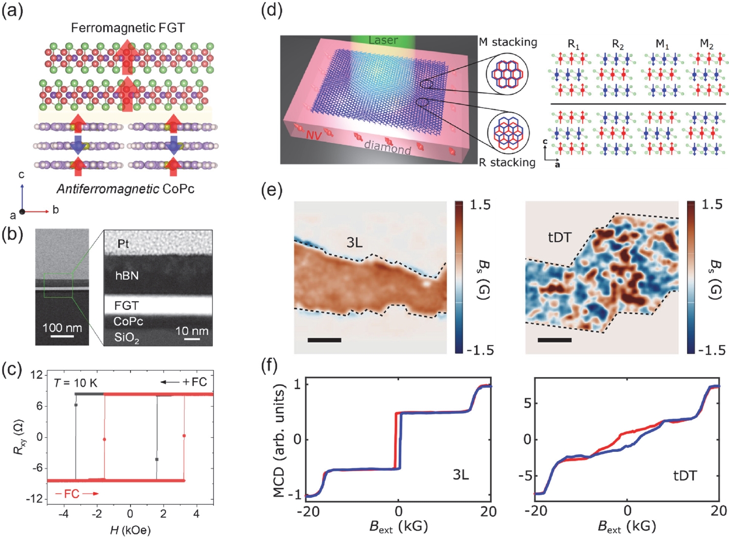
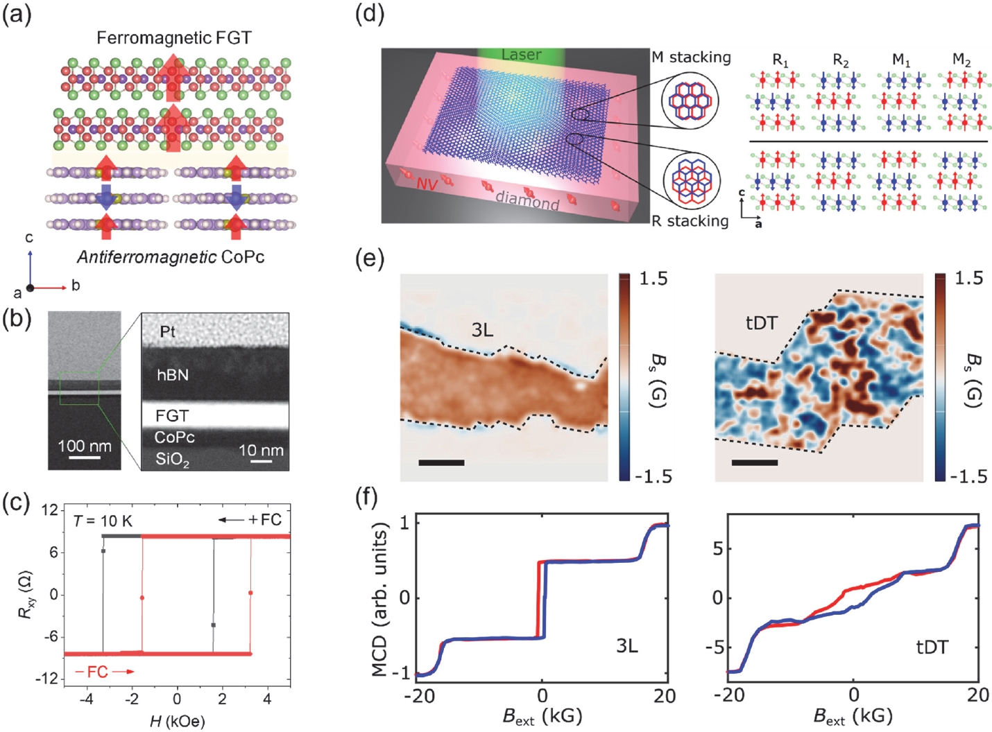
Another example is a heterostructure of an organic layer and a 2D vdW magnet (
Fig. 5(a)) [
28,
29]. When the vdW ferromagnetic Fe
3GeTe
2 meets an organic molecular layer, forming a hybrid interface, the interface dominates the overall magnetic properties of the heterostructure through interfacial exchange interaction. In this case, the Fe
3GeTe
2 activates antiferromagnetic order in the organic layer, resulting in exchange bias in the system.
Recently, twistronics has expanded the scope of material architecture in vdW systems, enabling electronic and magnetic properties to be controlled through the relative rotation between adjacent layers. For instance, when two CrI
3 layers are stacked with a relative twist angle, a long-period moiré pattern forms, producing spatially varying stacking configurations (
Fig. 5(d-f)) [
30]. As a result, the twisted CrI
3 structure exhibits newly formed magnetic domains and magnetic anisotropy. From a device perspective, twisted CrSBr heterostructures further demonstrate that twist engineering can be directly translated into spin-dependent transport functions. Orthogonally twisted CrSBr monolayers have exhibited multistep magnetization switching [
31], while twisted CrSBr bilayers enabled atomically thin all-antiferromagnetic tunnel junctions [
32].
3 Conclusion
In summary, materials engineering provides a practical framework for tailoring the magnetic properties of 2D vdW magnets beyond their intrinsic characteristics. Electrostatic engineering enables reversible control of carrier density, magnetic anisotropy, and interlayer exchange through dielectric, ferroelectric, floating, and ionic gates. Chemical engineering including intercalation and defect control offers a more persistent route for structural modifications and magnetic characteristics. Lattice engineering directly tunes magnetic properties by changing bond geometries and orbital overlap through strain and pressure. Symmetry engineering governed by atomic arrangements activates diode-like electrical responses, providing useful routes for electrical readout and rectification. Heterostructure engineering further expands the design strategy by combining 2D magnets with other layered materials, molecular layers, and twisted structures. Although these approaches are separately classified in this review, they are often coupled and give rise to synergies in material designs.
Further progress requires the broader application of engineering strategies to various classes of 2D vdW magnets, together with delicate optimization for stability, reproducibility, and scalability. By integrating multiple engineering strategies, 2D vdW magnets can be transformed into versatile material platforms for exploring novel magnetic phenomena and developing future electronic, spintronic, and multifunctional device applications.
Notes
-
Acknowledgement
This work was supported by the National Research Foundation of Korea (NRF) grant funded by the Korea government (MSIT) (RS-2026-25475074). This research was supported by the Commercialization Promotion Agency for R&D Outcomes (COMPA) grant funded by the Ministry of Science and ICT (MSIT) (RS-2023-00304743).
-
Conflict of Interest
The authors have no conflicts of interest to declare.
-
Author Contributions
Junhyeon Jo: Conceptualization, Methodology, Investigation, Data Curation, Writing - Original Draft, Writing - Review & Editing, Visualization, Funding acquisition.
Data Availability
Data available on request from the authors.
Fig. 1.(a,b) Electrostatic gating effects and hopping transport analysis on an antiferromagnetic semiconductor CrSBr flake. Reproduced in part from Ref. [
13] under the CC BY-NC-ND license. (c) Optical image of a 2D floating gate architecture on CrSBr. (d) Magnetism-dependent gate voltage sweep behavior, (e) gate-polarization-dependent magnetoresistance, and (f) gate pulse measurement for switching performance on the floating gated CrSBr. Reprinted in part with permission from Ref. [
15] under the Copyright 2024 American Chemical Society
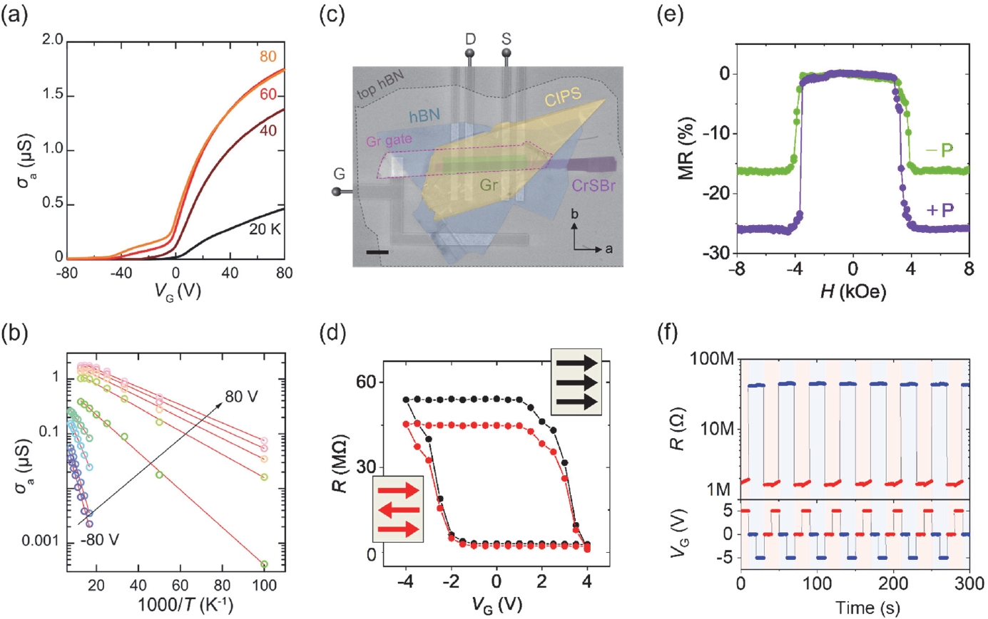
Fig. 2.(a) Mechanism of organic intercalation into antiferromagnetic MnPS3 through the molecule-dependent vacancy process. (b) Magnetization of a series of intercalated MnPS3. Reproduced in part with permission from Ref. [
17] under the Copyright 2024 Wiley-VCH GmbH. (c) Schematic image of intercalated CrSBr. (d) Temperature-dependent magnetization for CrSBr with intercalated molecules TMA and TPA, respectively. (e) Axis-dependent magnetization in TMA-intercalated CrSBr. Reprinted in part with permission from Ref. [
18] under the Copyright 2025 American Chemical Society
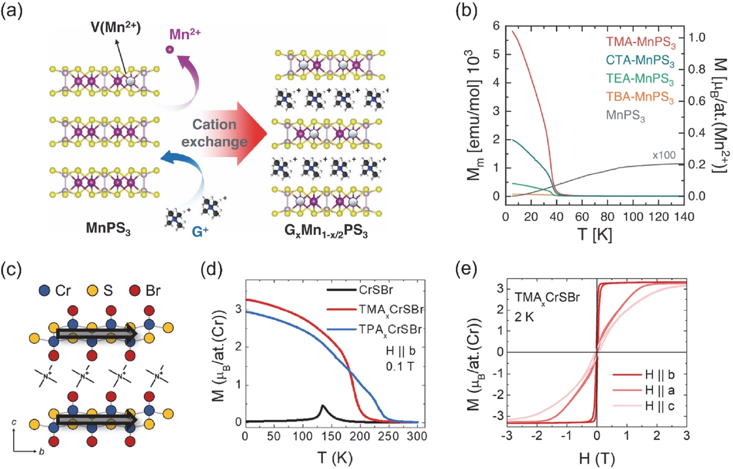
Fig. 3.(a) Schematic image for the method to apply strain to an Fe
3GeTe
2 flake on the flexible substrate. (b) Strain-dependent anomalous Hall responses of the Fe
3GeTe
2. (c) Enhancement of magnetic critical temperature of the strained Fe
3GeTe
2. Reproduced in part from Ref. [
21] under the CC BY-NC license. (d) Methodology to induce the strain effect on CrSBr. (e,f) Conductivity and magnetic anisotropy modification under strain on CrSBr. Reproduced in part with permission from Ref. [
22] under the Copyright 2020 Wiley-VCH GmbH
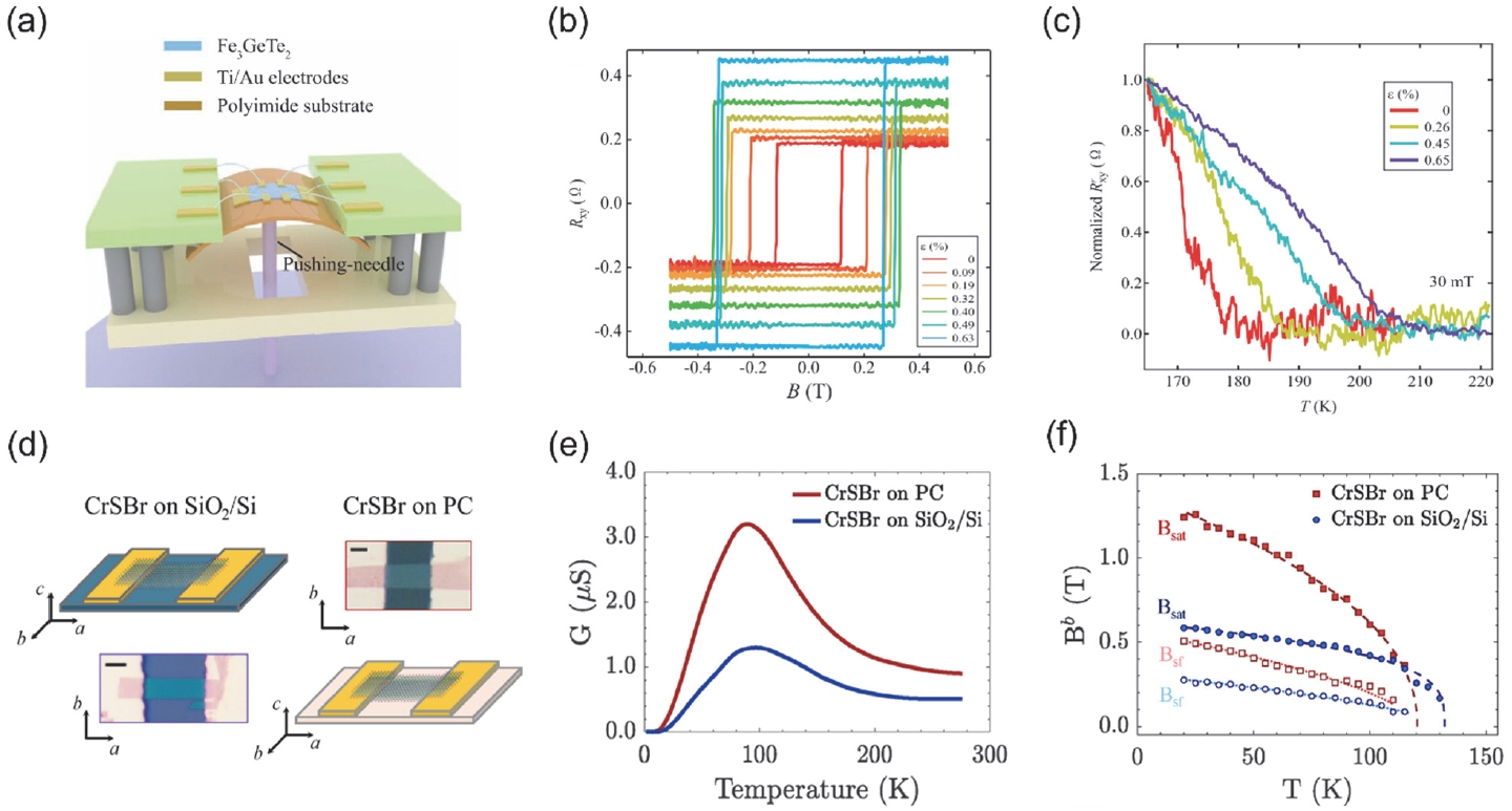
Fig. 4.(a-c) Schematic images of pristine CrSBr(1L), CrSBr(1L)/hBN, and CrSBr(2L)/hBN which show the symmetry control in CrSBr flakes using the hBN layer. (d-f) Nonlinear magnetoresistance of the structure in (a-c), exhibiting the electrical readout of the magnetic states by symmetry engineering. Reproduced in part with permission from Ref. [
26] under the Copyright 2025 Wiley-VCH GmbH
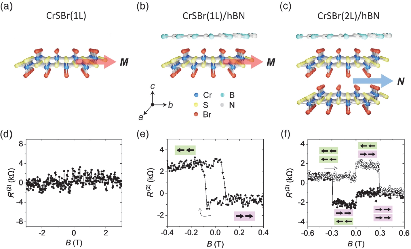
Fig. 5.(a) Schematic illustration of the heterostructure of 2D ferromagnet Fe
3GeTe
2 and molecule CoPc layers, activating antiferromagnetism in the CoPc. (b) Cross-sectional view of the heterostructure displaying clean interfaces. (c) Exchange bias effect in the Fe
3GeTe
2/CoPc. Reproduced in part with permission from Ref. [
28] under the Copyright 2022 Wiley-VCH GmbH. (d) Schematic images of twisted CrI
3 layers and their stacking configurations. (e) Images of magnetic stray fields from pristine trilayer and twisted trilayer, respectively. (f) MCD results without and with twist, respectively. Adapted from Ref. [
30] under the terms of the Creative Commons Attribution 4.0 International License (CC BY 4.0)
References
- 1. C. Gong, L. Li, Z. Li, H. Ji, A. Stern, Y. Xia, T. Cao, W. Bao, C. Wang, Y. Wang, Z. Q. Qiu, R. J. Cava, S. G. Louie, J. Xia, and X. Zhang, Nature, 546, 265 (2017). doi: https://doi.org/10.1038/nature22060
- 2. B. Huang, G. Clark, E. Navarro-Moratalla, D. R. Klein, R. Cheng, K. L. Seyler, D. Zhong, E. Schmidgall, M. A. McGuire, D. H. Cobden, W. Yao, D. Xiao, P. Jarillo-Herrero, and X. Xu, Nature, 546, 270 (2017). doi: https://doi.org/10.1038/nature22391
- 3. Y. Deng, Y. Yu, Y. Song, J. Zhang, N. Z. Wang, Z. Sun, Y. Yi, Y. Z. Wu, S. Wu, J. Zhu, J. Wang, X. H. Chen, and Y. Zhang, Nature, 563, 94 (2018). doi: https://doi.org/10.1038/s41586-018-0626-9
- 4. K. Z. Du, X. Z. Wang, Y. Liu, P. Hu, M. I. B. Utama, C. K. Gan, Q. Xiong, and C. Kloc, ACS Nano, 10, 1738 (2016). doi: https://doi.org/10.1021/acsnano.5b05927
- 5. E. J. Telford, A. H. Dismukes, K. Lee, M. Cheng, A. Wieteska, A. M. Bartholomew, Y. S. Chen, X. Xu, A. N. Pasupathy, X. Y. Zhu, C. R. Dean, and X. Roy, Adv. Mater., 32, 2003240 (2020). doi: https://doi.org/10.1002/adma.202003240
- 6. Y. Deng, Y. Yu, M. Z. Shi, Z. Guo, Z. Xu, J. Wang, X. H. Chen, and Y. Zhang, Science, 367, 895 (2020). doi: https://doi.org/10.1126/science.aax8156
- 7. G. Zhang, F. Guo, H. Wu, X. Wen, L. Yang, W. Jin, W. Zhang, and H. Chang, Nat. Commun., 13, 5067 (2022). doi: https://doi.org/10.1038/s41467-022-32605-5
- 8. J. Lee, J. Gu, W. Kim, J. E. Lee, W. Chao, K. S. Lee, Z. Qiu, M. Y. Im, and H. S. Han, Adv. Funct. Mater., 36, e16597 (2026). doi: https://doi.org/10.1002/adfm.202516597
- 9. C. Tan, J. Lee, S. G. Jung, T. Park, S. Albarakati, J. Partridge, M. R. Field, D. G. McCulloch, L. Wang, and C. Lee, Nat. Commun., 9, 1554 (2018). doi: https://doi.org/10.1038/s41467-018-04018-w
- 10. B. Huang, G. Clark, D. R. Klein, D. MacNeill, E. Navarro-Moratalla, K. L. Seyler, N. Wilson, M. A. McGuire, D. H. Cobden, D. Xiao, W. Yao, P. Jarillo-Herrero, and X. Xu, Nat. Nanotechnol., 13, 544 (2018). doi: https://doi.org/10.1038/s41565-018-0121-3
- 11. S. Jiang, J. Shan, and K. F. Mak, Nat. Mater., 17, 406 (2018). doi: https://doi.org/10.1038/s41563-018-0040-6
- 12. Z. Wang, T. Zhang, M. Ding, B. Dong, Y. Li, M. Chen, X. Li, J. Huang, H. Wang, X. Zhao, Y. Li, D. Li, C. Jia, L. Sun, H. Guo, Y. Ye, D. Sun, Y. Chen, T. Yang, J. Zhang, S. Ono, Z. Han, and Z. Zhang, Nat. Nanotechnol., 13, 554 (2018). doi: https://doi.org/10.1038/s41565-018-0186-z
- 13. F. Wu, I. Gutiérrez-Lezama, S. A. López-Paz, M. Gibertini, K. Watanabe, T. Taniguchi, F. O. von Rohr, N. Ubrig, and A. F. Morpurgo, Adv. Mater., 34, 2109759 (2022). doi: https://doi.org/10.1002/adma.202109759
- 14. E. J. Telford, A. H. Dismukes, R. L. Dudley, R. A. Wiscons, K. Lee, D. G. Chica, M. E. Ziebel, M. G. Han, J. Yu, S. Shabani, A. Scheie, K. Watanabe, T. Taniguchi, D. Xiao, Y. Zhu, A. N. Pasupathy, C. Nuckolls, X. Zhu, C. R. Dean, and X. Roy, Nat. Mater., 21, 754 (2022). doi: https://doi.org/10.1038/s41563-022-01245-x
- 15. J. Jo, S. Mañas-Valero, E. Coronado, F. Casanova, M. Gobbi, and L. E. Hueso, Nano Lett., 24, 4471 (2024). doi: https://doi.org/10.1021/acs.nanolett.4c00348
- 16. M. Tang, J. Huang, F. Qin, K. Zhai, T. Ideue, Z. Li, F. Meng, A. Nie, L. Wu, X. Bi, C. Zhang, L. Zhou, P. Chen, C. Qiu, P. Tang, H. Zhang, X. Wan, L. Wang, Z. Liu, Y. Tian, Y. Iwasa, and H. Yuan, Nat. Electron., 6, 28 (2023). doi: https://doi.org/10.1038/s41928-022-00882-z
- 17. D. Tezze, J. M. Pereira, D. Tutar, M. Ramos, J. Regner, P. Gargiani, F. Schiller, F. Casanova, A. Alegria, B. Martín-García, H. Sahin, Z. Sofer, M. Ormaza, L. E. Hueso, and M. Gobbi, Adv. Funct. Mater., 35, 2412771 (2025). doi: https://doi.org/10.1002/adfm.202412771
- 18. S. Ferreira-Teixeira, D. Tezze, M. Ramos, C. Álvarez-García, B. Bayındır, J. Jo, B. Martín-García, M. Ormaza, F. Casanova, S. Mañas-Valero, E. Coronado, H. Sahin, L. E. Hueso, and M. Gobbi, ACS Nano, 19, 36275 (2025). doi: https://doi.org/10.1021/acsnano.5c08747
- 19. M. Bonilla, S. Kolekar, Y. Ma, H. C. Diaz, V. Kalappattil, R. Das, T. Eggers, H. R. Gutierrez, M. H. Phan, and M. Batzill, Nat. Nanotechnol., 13, 289 (2018). doi: https://doi.org/10.1038/s41565-018-0063-9
- 20. W. Yu, J. Li, T. S. Herng, Z. Wang, X. Zhao, X. Chi, W. Fu, I. Abdelwahab, J. Zhou, J. Dan, Z. Chen, Z. Chen, Z. Li, J. Lu, S. J. Pennycook, Y. P. Feng, J. Ding, and K. P. Loh, Adv. Mater., 31, 1903779 (2019). doi: https://doi.org/10.1002/adma.201903779
- 21. Y. Wang, C. Wang, S. J. Liang, Z. Ma, K. Xu, X. Liu, L. Zhang, A. S. Admasu, S. W. Cheong, L. Wang, M. Chen, Z. Liu, B. Cheng, W. Ji, and F. Miao, Adv. Mater., 32, 2004533 (2020). doi: https://doi.org/10.1002/adma.202004533
- 22. E. Henríquez-Guerra, A. M. Ruiz, M. Galbiati, Á. Cortés-Flores, D. Brown, E. Zamora-Amo, L. Almonte, A. Shumilin, J. Salvador-Sánchez, A. Pérez-Rodríguez, I. Orue, A. Cantarero, A. Castellanos-Gomez, F. Mompeán, M. Garcia-Hernandez, E. Navarro-Moratalla, E. Diez, M. Amado, J. J. Baldoví, and M. R. Calvo, Adv. Mater., 2506695 (2025). doi: https://doi.org/10.1002/adma.202506695
- 23. T. Li, S. Jiang, N. Sivadas, Z. Wang, Y. Xu, D. Weber, J. E. Goldberger, K. Watanabe, T. Taniguchi, C. J. Fennie, K. F. Mak, and J. Shan, Nat. Mater., 18, 1303 (2019). doi: https://doi.org/10.1038/s41563-019-0506-1
- 24. Z. Zhang, N. Wang, N. Cao, A. Wang, X. Zhou, K. Watanabe, T. Taniguchi, B. Yan, and W. B. Gao, Nat. Commun., 13, 6191 (2022). doi: https://doi.org/10.1038/s41467-022-33705-y
- 25. N. Wang, D. Kaplan, Z. Zhang, T. Holder, N. Cao, A. Wang, X. Zhou, F. Zhou, Z. Jiang, C. Zhang, S. Ru, H. Cai, K. Watanabe, T. Taniguchi, B. Yan, and W. Gao, Nature, 621, 487 (2023). doi: https://doi.org/10.1038/s41586-023-06363-3
- 26. J. Jo, M. Suárez-Rodríguez, S. Mañas-Valero, E. Coronado, I. Souza, F. de Juan, F. Casanova, M. Gobbi, and L. E. Hueso, Adv. Mater., 37, 2419283 (2025). doi: https://doi.org/10.1002/adma.202419283
- 27. W. Zhao, Z. Fei, T. Song, H. K. Choi, T. Palomaki, B. Sun, P. Malinowski, M. A. McGuire, J. H. Chu, X. Xu, and D. H. Cobden, Nat. Mater., 19, 503 (2020). doi: https://doi.org/10.1038/s41563-020-0620-0
- 28. J. Jo, F. Calavalle, B. Martín-García, D. Tezze, F. Casanova, A. Chuvilin, L. E. Hueso, and M. Gobbi, Adv. Mater., 34, 2200474 (2022). doi: https://doi.org/10.1002/adma.202200474
- 29. M. Sharma, J. Jo, G. Avedissian, B. Bayindir, J. Kang, H. Sahin, F. Casanova, M. Gobbi, and L. E. Hueso, ACS Appl. Electron. Mater., 7, 9204 (2025). doi: https://doi.org/10.1021/acsaelm.5c01598
- 30. M. Huang, Z. Sun, G. Yan, H. Xie, N. Agarwal, G. Ye, S. H. Sung, H. Lu, J. Zhou, S. Yan, S. Tian, H. Lei, R. Hovden, R. He, H. Wang, L. Zhao, and C. R. Du, Nat. Commun., 14, 5259 (2023). doi: https://doi.org/10.1038/s41467-023-40543-z
- 31. C. Boix-Constant, S. Jenkins, R. Rama-Eiroa, E. J. Santos, S. Mañas-Valero, and E. Coronado, Nat. Mater., 23, 212 (2024). doi: https://doi.org/10.1038/s41563-023-01735-6
- 32. Y. Chen, K. Samanta, N. A. Shahed, H. Zhang, C. Fang, A. Ernst, E. Y. Tsymbal, and S. S. Parkin, Nature, 632, 1045 (2024). doi: https://doi.org/10.1038/s41586-024-07818-x