ABSTRACT
The development of a large-area solution process for CuO nanowires, which are promising p-type thin film transistors (TFT) channel materials, is required. To overcome the limitations of the existing high-vacuum and high-cost deposition process, a large-area Cu nanowire network was formed on the substrate using the Mayer rod coating method, and a CuO channel was implemented by subsequent thermal annealing. Consequently, p-type TFT with an on/off current ratio of 1.4×10⁴ and a field-effect mobility µFE≈10-4 cm2/(V⋅s). was fabricated and optimized. X-ray diffraction (XRD) and X-ray photoelectron spectroscopy (XPS) analyses showed that the sample annealed at 200°C exhibited an incomplete oxidation state with a mixed Cu/Cu2O phase and a high fraction of M-OH species (58.78%), resulting in a low on/off current ratio (≈1.2). In contrast, annealing at 450°C leads to a CuOdominant phase, where the fraction of lattice oxygen(O1) increases to 31.11% and the oxygen vacancy (VO) component increases to 7.15%, indicating a significant improvement in hole concentration and charge transport. These phase transitions and surface chemical changes are identified as the key mechanisms for the enhanced TFT switching characteristics. The low-cost, large-area Mayer rodbased solution process proposed in this study provides a basic process platform for p-type TFTs applicable to flexible wearables and display technologies and suggests the possibility of commercialization through additional optimization of bias stability in the future.
-
KEYWORDS: CuO, Nanowire, Mayer rod, XPS, XRD
구리 산화물(CuO)은 우수한 p형 반도체 특성, 가시광 영역을 넓게 흡수하는 밴드갭(약 1.2–1.9 eV), 높은 정공 이동도, 그리고 풍부한 자연 결함 구조로 인해 박막 트랜지스터(TFT) 채널 물질로 활발히 연구되고 있다[
1–
3]. 특히, CuO는 나노 와이어(nanowire)나 나노섬유(nanofiber)와 같은 1차원 구조 형태로 많이 활용되어, 전자 구속 효과 및 높은 비표면적으로 향상된 전하 이동도와 결정 결함 영향 감소라는 장점을 보유하고 있다. 이러한 1차원 나노구조는 박막 형태에 비해 소자 성능 향상에 중요한 기여를 하며, TFT 채널에 적합하다[
4–
6].
한편 기존 CuO 박막 TFT는 고진공 증착, 고온 공정, 복잡한 패터닝이 요구되어 비용과 확장성 면에서 한계가 분명하다[
7–
14]. 이에 반해 본 연구는 대면적 및 저비용 습식 공정인 Mayer rod 코팅법을 활용하여 균일하고 고연속성의 Cu 나노 와이어 네트워크를 손쉽게 형성하고, 후속 산화 공정으로 최적의 CuO 활성층을 구현하고자 하였다. Mayer rod 코팅법은 간단한 장비만으로도 두께·밀도 제어가 용이하며 대면적 패널 제작에 적합한 경제적 공정으로 2차원 박막 제조분야에서 이미 확립되어 있다[
15–
17]. 이를 CuO 나노와이어 기반 TFT에 접목함으로써 기존 고가·고진공 공정에 비해 크게 공정 효율성을 개선할 수 있을 것으로 기대된다.
본 연구에서는 열처리 온도에 따른 CuO 상 전이 및 표면 화학 변화를 XRD와 XPS로 분석하고, 다양한 온도 조건에서 TFT 성능 변화를 체계적으로 평가하였다. 이를 통해 단순하고 경제적인 대면적 Mayer rod 기반 습식 공정으로 제조한 CuO 나노와이어 TFT는 약 1.4 × 10⁴의 On/Off 전류비를 달성하여 기본적인 전기적 특성 확보가 가능함을 입증하고, 기존의 CuO 기반 p형 TFT 성능과 비교했을 때 경쟁력 있는 수준에 도달함을 보이고자 한다.
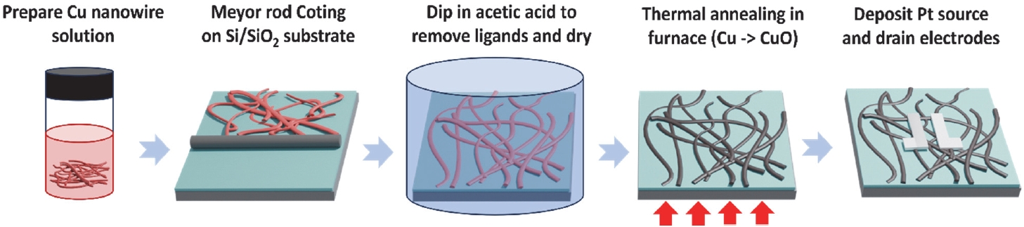
그림 1은 수열합성법으로 만들어진 CuO 나노와이어 기반 TFT의 공정 모식도를 나타낸다.
Cu 나노와이어는 HDA(hexadecylamine) 기반 수열합성법으로 제조하였으며, 상세한 제작 방법은 참고문헌[
16,
18]에 기술되어 있다.
기판으로는 Si(100) 웨이퍼(열산화 SiO₂, 300 nm)를 사용하였다. 공정 전에 기판은 아세톤, IPA, 증류수에서 각각 10 min 초음파 세척 후 건조하였고, 잔류 결함 제거를 위해 500°C에서 1 h furnace annealing을 수행하였다.
50 mg/ml 농도의 Cu 나노와이어 용액을 Mayer rod(#8, RD Specializes)를 이용하여 기판 위에 코팅하였다. 그 후 Cu나 노와이어를 감싼 유기물(HDA) 제거를 위해 acetic acid 용액에 10 s 동안 침지 후 히팅 건으로 건조하였다. 코팅된 기판을 Cu 나노와이어를 Furnace에서 200°C 및 450°C로 각각 1 h annealing하여 CuxO 활성층을 형성하였다. 마지막으로 Bottom gate 구조로 채널 폭(w) = 1,000 μm 채널 길이(L) = 50 μm가 되도록 shadow mask를 이용해 TFT 구조에 RF magnetron sputtering으로 Pt (100 nm) S/D 전극을 증착하였다. 전기적 특성은 Keithley 4200-SCS로 측정하였으며, 구조 분석은 FE-SEM (Hitachi S-4700), XRD (BrukerD8 ADVANCE, Cu Kα), XPS (Hybrid system with UPS/Raman, Al Kα, C 1s 284.8 eV 기준)을 사용하였다.
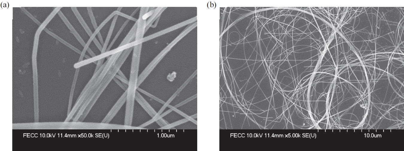
그림 2는 수열합성법으로 합성된 Cu 나노와이어의 형상을 FE–SEM으로 관찰한 결과를 나타낸다. 무작위로 선택한 50개 나노와이어를 통계적으로 분석한 결과, 평균 직경은 약 55 ± 10 nm, 평균 길이는 수십~수백 μm 이상으로 측정되었으며, 종횡비는 3,000 이상으로 확인되었다.
이러한 고종횡비 Cu 나노와이어는 일반적인 투명 전극 소재로 널리 사용되는 Ag 나노와이어(종횡비 약 500~1,000 수준) [
19,
20] 대비 큰 종횡비를 가져, Mayer rod 코팅 후 소스–드레인 전극 사이에 연속적인 전도 경로를 형성하기에 유리하다. Mayer rod 코팅에 의해 형성된 Cu 나노와이어 네트워크는 채널 전 영역에 걸쳐 균일한 percolation 경로를 제공하여 후속 산화 공정 이후 전하 수송을 촉진하고, TFT의 전기적 성능 향상에 기여하는 것으로 판단된다. 또한 Mayer rod 공정은 공정 조건을 단순화하면서도 대면적 기판에 대한 균일 코팅이 가능하다는 장점을 가지므로, 본 Cu
xO 나노와이어 기반 TFT 구조를 확장성 있는 공정으로 구현하는 데 적합한 기술로 판단된다.
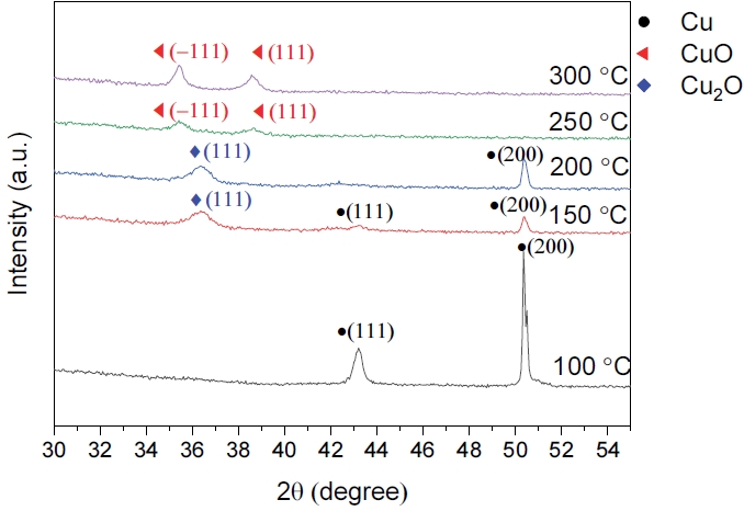
그림 3은 100–300°C 범위에서 열처리한 Cu
xO 나노와이어의 X선 회절(XRD) 패턴을 나타낸다. 100°C 열처리 소자에서는 금속 Cu(111) 및 (200) 피크만 관찰되어, 해당 온도에서는 나노와이어가 거의 산화되지 않은 상태임을 알 수 있다. 150°C에서는 Cu₂O(111) 피크가 처음으로 출현함과 동시에 Cu(200) 피크만 잔존하여, 금속 Cu에서 Cu₂O로의 초기 산화가 개시된 것으로 해석된다. 200°C에서는 Cu₂O(111) 피크가 유지되는 반면 Cu(111) 피크가 소실되어 금속 상이 상당 부분 소멸하고(Cu(200)은 여전히 존재) 산화가 더욱 진전된 상태임을 시사한다. 250–300°C에서는 CuO(–111) 및 (111) 피크만 뚜렷하게 관찰되며 Cu₂O 관련 피크는 사라져, Cu₂O에서 CuO로의 상 전이가 본격적으로 진행되어 CuO 상이 우세한 구조로 전환되었음을 알 수 있다.
본 연구에서는 300°C를 초과하는 온도 영역에 대한 XRD 데이터는 확보하지 못하였으므로, 300°C 이상의 열처리 시편에 대해 XRD만으로 CuO 단일상 또는 우세상을 단정할 수 없다. 다만 250–300°C에서 CuO 회절 피크만 관찰되는 점과 후술하는 O 1s 및 Cu 2p XPS 분석에서 확인된 CuO 격자 산소 및 Cu
2+ 성분 비율의 증가를 고려할 때, 300°C 이상 고온 열처리 조건에서도 보다 CuO 우세상이 형성되는 경향을 갖는 것으로 판단된다[
21,
22].
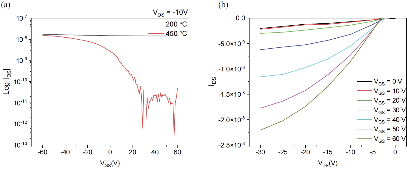
그림 4(a)는 200℃와 450℃에서 열처리한 Cu
xO 나노와이어 TFT의 Transfer 특성을 비교한 것이며, 200℃ 열처리 소자는 transfer 특성에서 게이트 전압 변화에 따른
IDS의 변화가 거의 나타나지 않아 On/Off 전류비가 약 1.2에 불과하고 문턱 전압 및 곡선의 형상이 불명확하여 p형 트랜지스터로서의 동작이 매우 미약하다. 이는 앞선 XRD 분석에서 확인된 바와 같이 불완전한 산화로 인한 Cu/Cu
2O 혼상 구조와 다수의 계면 트랩 및 산소 결함이 존재하여 전도 경로를 불연속적으로 만들고 캐리어 수송을 제한하기 때문으로 해석된다.
반면, 450℃ 열처리 소자는 transfer 특성에서 VGS가 +60 V에서 −60 V로 감소함에 따라 |IDS|가 10-12 A 수준에서 10-8 A 수준까지 3~4자릿수 이상 증가하는 뚜렷한 게이트 전압 의존성을 보인다. 문턱전압(Vth)은 약 +20 V로 추출되며 그 이하의 전압에서 채널이 활성화 상태가 되어 P형 트랜지스터 특성이 분명히 나타난다. 다만 비교적 높은 Vth로 인하여 완전한 Off 상태를 얻기 위해서는 높은 양의 게이트 전압이 필요하다는 한계가 존재한다. 이러한 높은 Vth는 열처리 과정에서 형성된 게이트 절연막/채널 계면 트랩 및 고정 전하, 그리고 두꺼운 SiO₂ (300 nm) 게이트 절연막에 기인한 것으로 판단되며, 실용적인 저전압 구동을 위해서는 추가적인 공정, 계면 최적화를 통해 Vth를 0 V 근처로 조정할 필요가 있다.
그림 4(b)의 게이트 전압을 0 V에서 −60 V까지 −10 V 간격으로 변화시키며 측정한 Output 특성에서는 낮은
VDS 구간에서는 선형적인 전류 증가와 함께
VDS의 값이 커짐에 따라 전류 증가폭이 둔화되며 포화 상태에 도달하려는 경향을 보인다. 비록 나노와이어의 네트워크 구조의 기생 저항 등의 의해 완벽한 전류 포화는 일어나지 않았으나, 고온 열처리를 통해 결함이 적은 결정성 CuO 우세상이 형성됨에 따라 P형 트랜지스터로써 기본적인 전하 수 수송 경로가 확보되고 스위칭 특성이 유의미하게 개선된 결과로 판단된다.
Field-effect mobility (µFE)는 선형 영역에서 다음 식을 이용하여 추출하였다:
여기서 L과 W는 각각 채널 길이(50 μm)와 폭(1,000 μm) CDX는 게이트 절연막의 단위면적당 정전용량 ∂IDS∂VGS는 transfer curve 의 선형 구간 기울기를 의미한다. 450℃ 소자의 µFE 는 약 10-4 cm2/(V⋅s) 수준으로 평가되며, 이는 두꺼운 SiO₂ 게이트 절연막과 나노네트워크 구조에서 기인한 큰 접촉 저항에 의해 낮은 값이 나왔다고 볼 수 있다. 그럼에도 불구하고 열처리 온도에 따른 상전이를 통해 Cu /Cu₂O 혼상에서 CuO 상으로 전환되면서 전하 수송 경로가 정비되고 On/Off 전류비가 200°C 열처리 소자에 비해 수 자릿수 이상 향상되는 등 스위칭 특성이 크게 개선되었음을 확인할 수 있다.
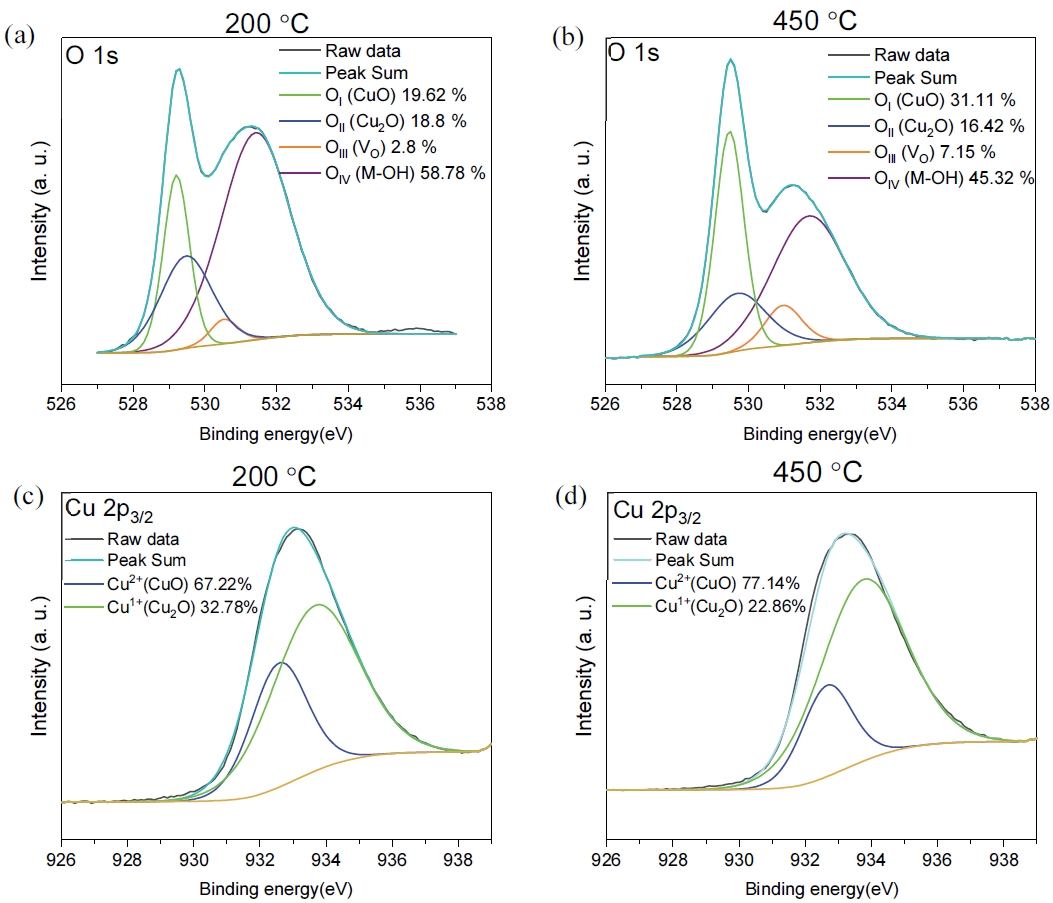
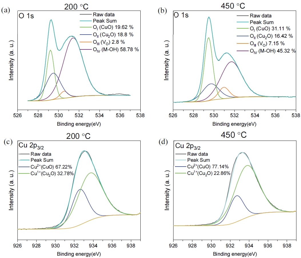
그림 5(a), (b)는 200°C와 450°C에서 열처리한 Cu
xO 나노와이어의 O 1s XPS 스펙트럼을 나타내며, 피크 분해를 통해 네 가지 성분(O1: CuO 격자 산소, O2: Cu₂O 격자 산소, O3: 산소 빈자리(V
O), O4: 흡착수산기(M–OH))으로 구분하였다. 200°C 열처리 소자의 경우, O4 (M–OH) 성분이 58.78%로 가장 큰 비중을 차지하고 O1 (CuO 격자 산소)이 19.62%, O2 (Cu₂O)가 18.80%, O3 (V
O)가 2.80%로 나타나, 표면에 수산기 및 흡착종이 다수 존재하는 불완전 산화 상태임을 보여준다.
450°C 열처리 소자에서는 O1 (CuO 격자 산소) 비율이 31.11%로 유의미하게 증가하고 O4 (M–OH)는 45.32%로 감소하였으며, O2 (Cu₂O)는 16.42%로 소폭 감소, O3 (V
O)는 7.15%로 증가하였다. 이와 같은 조성 변화는 열처리 온도 상승에 따라 표면 수산기 및 흡착종이 제거되고 CuO 격자 산소가 보다 우세해지는 경향을 반영하며, XRD에서 관찰된 Cu/Cu₂O 혼상에서 CuO 상 우세해지는 상전이 경향과 정성적으로 일치한다. 200°C 열처리소자에서 높은 M–OH 성분은 계면 및 벌크 내 전자 트랩 밀도를 증가시켜 낮은 On/Off 전류비(≈1.2)와 불안정한 전기적 특성을 유발하는 요인으로 작용하는 반면, 450°C 열처리 소자에서 관찰된 CuO 격자 산소 비율 증가는 구조적 결함을 감소시켜 전하 산란을 억제하고 동시에 산소 빈자리(O3) 증가는 CuO 내에서 정공(Hole)을 생성하는 도펀트 역할을 한다[
13,
14]. 이러한 결함 감소와 정공 농도의 증가는 450°C 열처리 소자에서 관찰된 On/Off 전류비 향상과 모빌리티 증가 등 스위칭 개선의 핵심 메커니즘으로 해석된다. 추가적으로 Cu 2p
3/2 스펙트럼 피팅 결과(
그림 5(c), (d)), 200°C와 450°C 시편 모두에서 Cu
+/Cu
2+ 혼상 구조가 관찰되며 Cu
2+(CuO) 성분이 우세하고, 450°C 열처리소자에서 Cu
2+ 비율이 증가하는 경향을 보여 O 1s 및 XRD 분석에서 관찰된 CuO 우세상으로의 전이와 정합된다.
본 연구에서는 수열합성법으로 고종횡비 Cu 나노와이어를 합성하고 Mayer rod 코팅법을 통해 균일한 네트워크를 형성한 후, 열처리 온도(200°C 및 450°C)를 통해 CuxO 나노와이어 네트워크를 형성하고 이를 채널층으로 하는 P형 CuxO 나노와이어 TFT를 구현하였다. XRD 패턴 분석 및 O 1s, Cu 2p3/2 XPS 스펙트럼 분석을 통해 열처리 온도에 따라 Cu/Cu2O/CuO 상의 상대적 비율과 표면 산소 화학 상태가 변화하며, 이에 따라 TFT의 µFE, Vth, On/Off 전류비가 변화하는 메커니즘을 체계적으로 규명하였다. 제조된 450°C 열처리 소자는 µFE(10-4 cm2/(V⋅s)) 및 Vth(+20 V) 측면에서 기존 용액 공정 CuxO 박막 TFT에서 보고된 µFE (10-4~10-2 cm2/(V⋅s))와 비교할 때 범위 하한에 해당하는 비교적 낮은 전기적 특성을 보이는 한계가 있다. 그럼에도 불구하고, 본 소자는 고진공 기반의 박막 증착 및 진공 어닐링 공정없이 Mayer rod 코팅법을 이용한 비교적 단순한 용액 공정만으로 CuxO 나노와이어 네트워크 채널을 형성할 수 있는 공정적 장점을 갖는다. 특히 Mayer rod 코팅법은 롤투롤 및 대면적 코팅과 양산 공정으로의 확장이 용이한 공정으로 이러한 Mayer rod 공정과 나노와이어 네트워크 구조를 결합한 본 연구의 CuO 나노와이어 채널은 대면적, 스케일러블 구현 및 디스플레이 패널 공정과의 호환성, 플렉서블 기판으로의 확장 가능성 측면에서 잠재력을 지닌다고 판단된다. 향후 게이트 절연막/채널 계면 트랩 저감, high-k 절연막 도입 및 네트워크 밀도/접촉 최적화와 같은 추가연구를 통해 µFE와 Vth을 개선한다면, 본 연구에서 제시한 Mayer rod 기반 CuO 나노와이어 TFT는 저비용, 대면적 P 형 산화물 TFT 개발의 중요한 기반이 될 것으로 기대된다.
Notes
-
Conflict of Interest
The authors have no conflicts of interest to declare.
-
Author Contributions
Jaeheung Im: Writing-Original Draft, Writing-Review & Editing, Visualization, and Supervision.
Data Availability
Data available within the article or its supplementary materials.
Fig. 1.Schematic illustration of the fabrication process for CuO NW TFTs on SiO2/Si
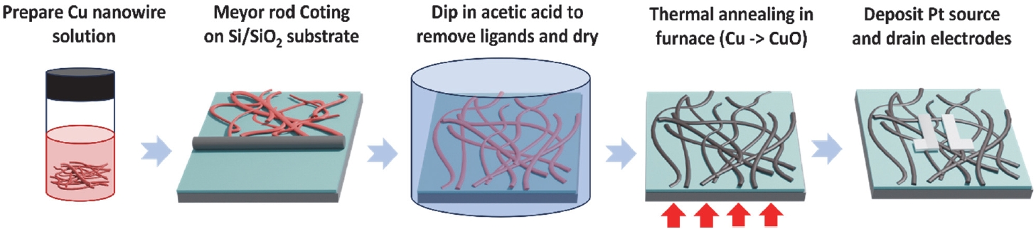
Fig. 2.Fe-SEM images of synthesized Cu NWs different scale: (a) scale bar = 1 μm, (b) scale bar = 10 μm
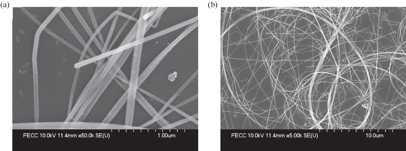
Fig. 3.XRD patterns of CuxO NWs after annealing at different temperatures
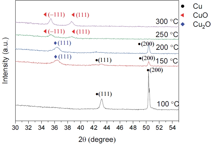
Fig. 4.Electrical characteristics of CuO nanowire TFTs: (a) transfer characteristics of devices annealed at 200°C and 450°C and (b) output characteristics of the device annealed at 450°C
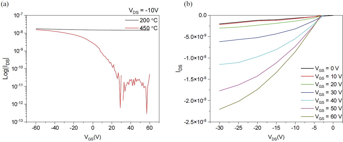
Fig. 5.XPS spectra of CuxO nanowire networks annealed at different temperatures: (a) O 1s at 200°C, (b) O 1s at 450°C, (c) Cu 2p3/2 at 200°C, and (d) Cu 2p3/2 at 450°C
References
- 1. Z. Wang, P. K. Nayak, J. A. Caraveo‐Frescas, and H. N. Alshareef, Adv. Mater., 28, 3831 (2016). doi: https://doi.org/10.1002/adma.201503080
- 2. H. A. Al-Jawhari, Mater. Sci. Semicond. Process., 40, 241 (2015). doi: https://doi.org/10.1016/j.mssp.2015.06.063
- 3. H. A. Al‐Jawhari, Adv. Electron. Mater., 8, 2100893 (2022). doi: https://doi.org/10.1002/aelm.202100893
- 4. L. Liao, B. Yan, Y. F. Hao, G. Z. Xing, J. P. Liu, B. C. Zhao, Z. X. Shen, T. Wu, L. Wang, J. T. L. Thong, C. M. Li, W. Huang, and T. Yu, Appl. Phys. Lett., 94, 113106 (2009). doi: https://doi.org/10.1063/1.3097029
- 5. C. Florica, A. Costas, A. G. Boni, R. Negrea, L. Ion, N. Preda, L. Pintilie, and I. Enculescu, Appl. Phys. Lett., 106, 223501 (2015). doi: https://doi.org/10.1063/1.4921914
- 6. S. Raveesh, V. K. S. Yadav, and R. Paily, IEEE Trans. Nanotechnol., 22, 184 (2023). doi: https://doi.org/10.1109/TNANO.2023.3262279
- 7. S. Ghosh, D. K. Avasthi, P. Shah, V. Ganesan, A. Gupta, D. Sarangi, R. Bhattacharya, and W. Assmann, Vacuum, 57, 377 (2000). doi: https://doi.org/10.1016/S0042-207X(00)00151-2
- 8. Z. Q. Yao, S. L. Liu, L. Zhang, B. He, A. Kumar, X. Jiang, W. J. Zhang, and G. Shao, Appl. Phys. Lett., 101, 042114 (2012). doi: https://doi.org/10.1063/1.4739524
- 9. W. Maeng, S. H. Lee, J. D. Kwon, J. Park, and J. S. Park, Ceram. Int., 42, 5517 (2016). doi: https://doi.org/10.1016/j.ceramint.2015.12.109
- 10. P. K. Ooi, S. S. Ng, M. J. Abdullah, H. Abu Hassan, and Z. Hassan, Mater. Chem. Phys., 140, 243 (2013). doi: https://doi.org/10.1016/j.matchemphys.2013.03.028
- 11. Y. Yang, J. Yang, W. Yin, F. Huang, A. Cui, D. Zhang, W. Li, Z. Hu, and J. Chu, Appl. Surf. Sci., 481, 632 (2019). doi: https://doi.org/10.1016/j.apsusc.2019.03.130
- 12. K. C. Sanal, L. S. Vikas, and M. K. Jayaraj, Appl. Surf. Sci., 297, 153 (2014). doi: https://doi.org/10.1016/j.apsusc.2014.01.109
- 13. W. K. Min, S. P. Park, H. J. Kim, J. H. Lee, K. Park, D. Kim, K. W. Kim, and H. J. Kim, ACS Appl. Mater. Interfaces, 12, 24929 (2020). doi: https://doi.org/10.1021/acsami.0c01530
- 14. M. Napari, T. N. Huq, D. J. Meeth, M. J. Heikkilä, K. M. Niang, H. Wang, T. Iivonen, H. Wang, M. Leskelä, M. Ritala, A. J. Flewitt, R. L. Z. Hoye, and J. L. MacManus-Driscoll, ACS Appl. Mater. Interfaces, 13, 4156 (2021). doi: https://doi.org/10.1021/acsami.0c18915
- 15. K. Triyana and E. Suharyadi, IOP Conf. Ser. Mater. Sci. Eng., 202, 012055 (2017). doi: https://doi.org/10.1088/1757-899X/202/1/012055
- 16. T. H. Duong and H. C. Kim, Ind. Eng. Chem. Res., 57, 3076 (2018). doi: https://doi.org/10.1021/acs.iecr.7b04709
- 17. L. Zhou, M. Yu, L. Yao, and W. Y. Lai, Adv. Eng. Mater., 24, 2101558 (2022). doi: https://doi.org/10.1002/adem.202101558
- 18. P. Tran, N. H. Tran, and J. H. Lee, Sci. Rep., 12, 8967 (2022). doi: https://doi.org/10.1038/s41598-022-13167-4
- 19. J. Liang, K. Tong, and Q. Pei, Adv. Mater., 28, 5986 (2016). doi: https://doi.org/10.1002/adma.201600772
- 20. Q. Xue, W. Yao, J. Liu, Q. Tian, L. Liu, M. Li, Q. Lu, R. Peng, and W. Wu, Nanoscale Res. Lett., 12, 480 (2017). doi: https://doi.org/10.1186/s11671-017-2259-6
- 21. L. De Los Santos Valladares, D. H. Salinas, A. B. Dominguez, D. A. Najarro, S. I. Khondaker, T. Mitrelias, C. H. W. Barnes, J. A. Aguiar, and Y. Majima, Thin Solid Films, 520, 6368 (2012). doi: https://doi.org/10.1016/j.tsf.2012.06.043
- 22. J. Jang, S. Chung, H. Kang, and V. Subramanian, Thin Solid Films, 600, 157 (2016). doi: https://doi.org/10.1016/j.tsf.2016.01.036
Citations
Citations to this article as recorded by